Redraw the echo hello-world board and add at least a button and LED with current-limiting resistor or design your own.
Learning Outcomes
Select and use software for circuit board design.
Demonstrate workflows used in circuit board design.
Software
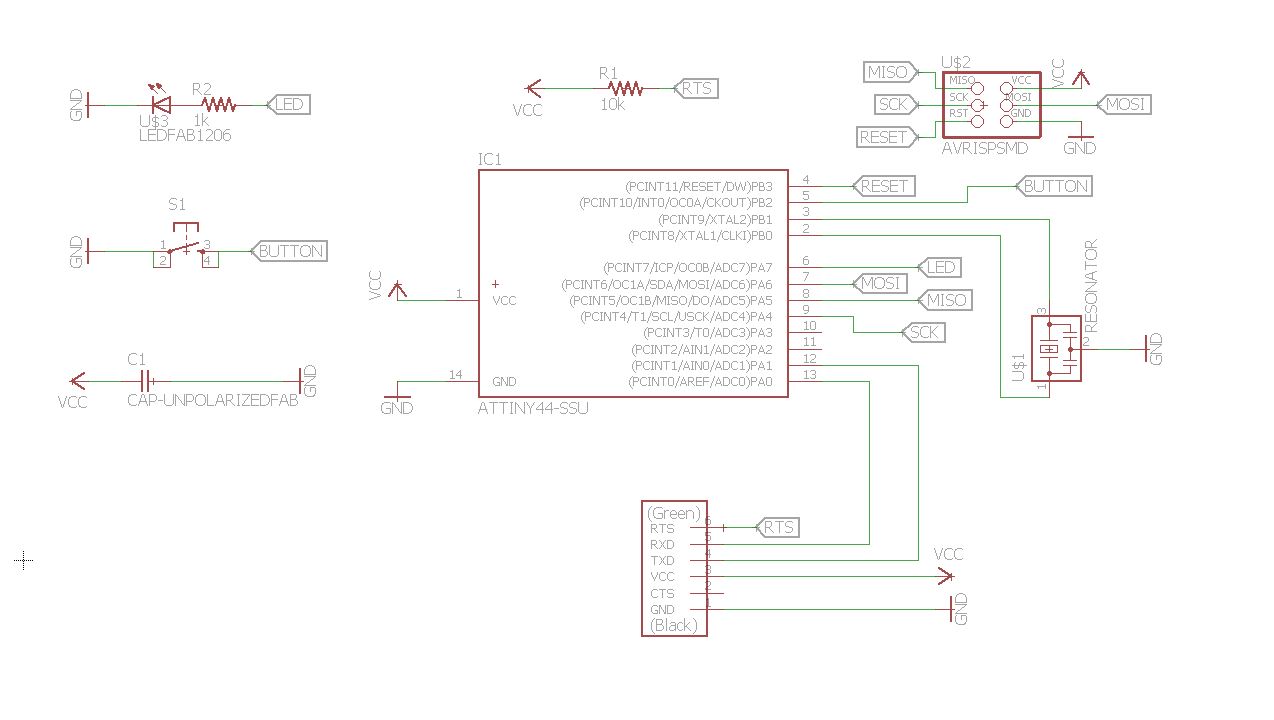
For this weeks assignment we were tasked in redrawing the Echo Hello-World board and add in at least one button and an LED. For this assignment I chose the program Eagle. This program allows you to add in components from different libraries and create your connections to each component. It also allows you to lay out your board so that you can create an image for milling. Opening Eagle, I realized I needed the right library to add in the correct components for the Echo Hello-World board. The library that I downloaded was the fab.lbr which contained each component for the Hello-World board. The following list are the components for the Echo Hello-World board with a button and LED:
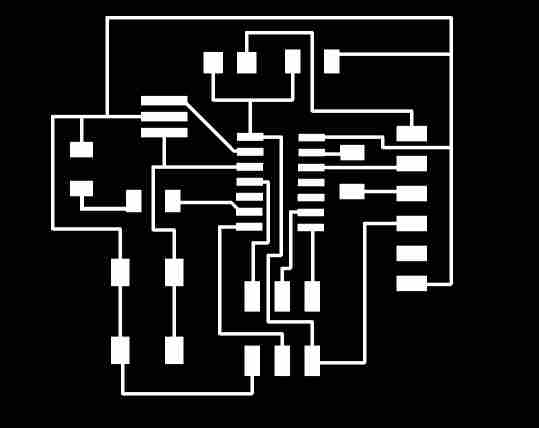
Using Eagle, I was able to layout each of these components in their schematic design layout. In this schematic design, Eagle allows you to create the right connections using wires and naming conventions to create your connections to each component. The final schmatic layout is shown in Figure 1.
Figure 1: Schematic of Echo Hello-World Board made in Eagle
After seeing that the right connections were made for each component, the schematic was ready to be made into a board. In the board layout within Eagle the pads are seen for each component as well as which pad connects to the other components. I started out by placing the components in a way I thought would be a good layout. Using the autorouter feature in Eagle, it routed the connections to each component in the best way it thought possible. Red routes mean it is a direct connection and the blue means it is not connected and needs to be jumped. This process took a lot of iterations for me until I was able find the best path without any jumps. Steven Fett then found a SCR code online to run within Eagle that takes away the description of the components and leaves some outlines on the board. Using Notepad, I entered he following code and saved it as a .scr file:
DISPLAY ALL
RATSNEST
DISPLAY None
DISPLAY Bottom Pads Vias
EXPORT IMAGE /mnt/slug_common/progs/!8051/!plosaky/!eagle_export.png MONOCHROME 600;
DISPLAY Top Unrouted Dimension tPlace bPlace
For my .scr code, I removed the EXPORT IMAGE and MONOCHROME line since I did not need these lines of code. After running this code, I exported the board layout as a picture and opened it in Paint. Using tools in Paint, I removed everything that wasn't needed to mill out my board (e.g. Resistor outlines, Button, line connections, etc). The following video shows this whole process during one of my iterations:
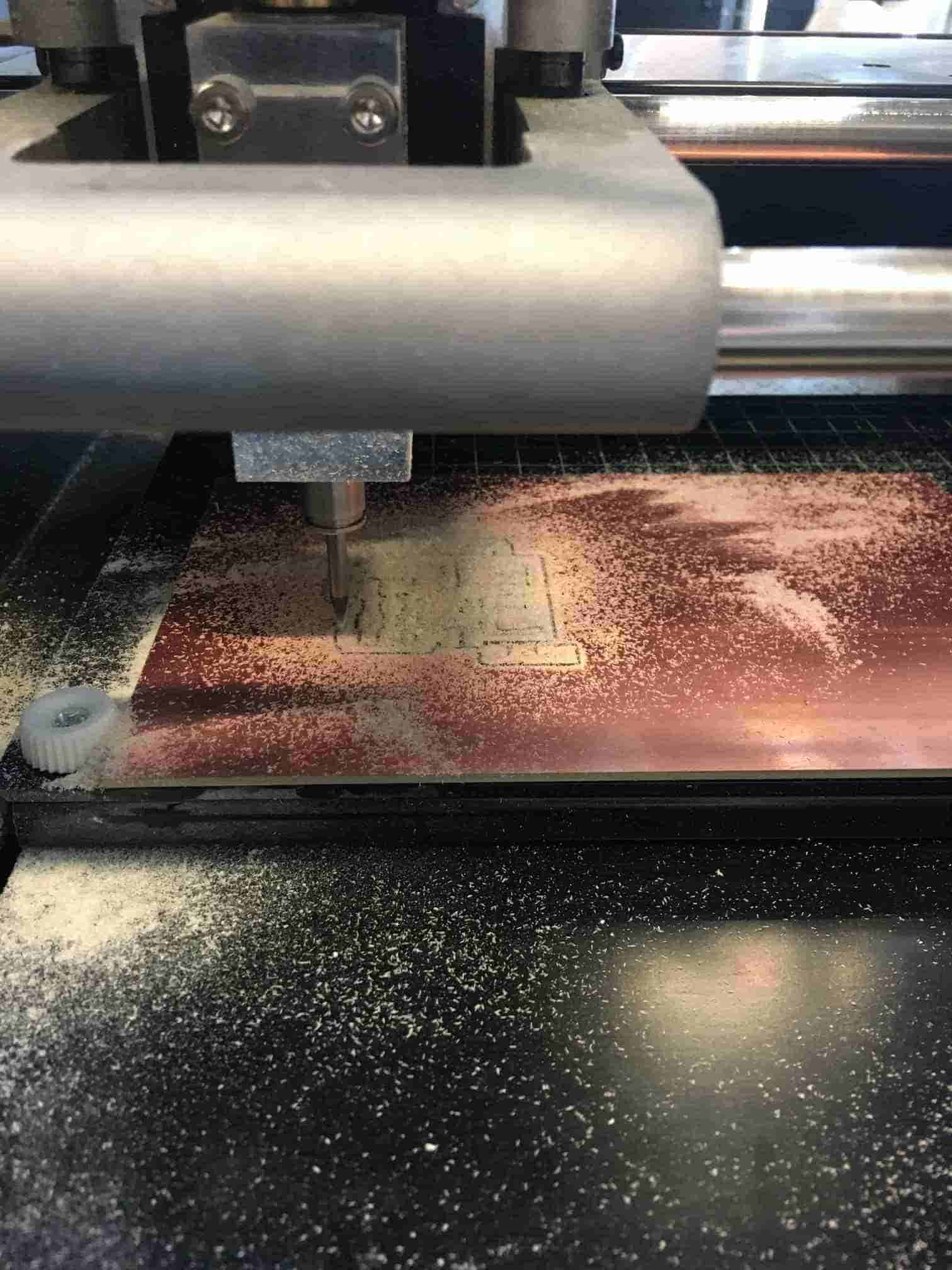
Using the same process as described in Week 4 I was able to cut out my first board as shown in Figure 2 and 3.
Figure 2: Milling Out Board
Figure 3: Finished Board after Milling
Troubleshooting
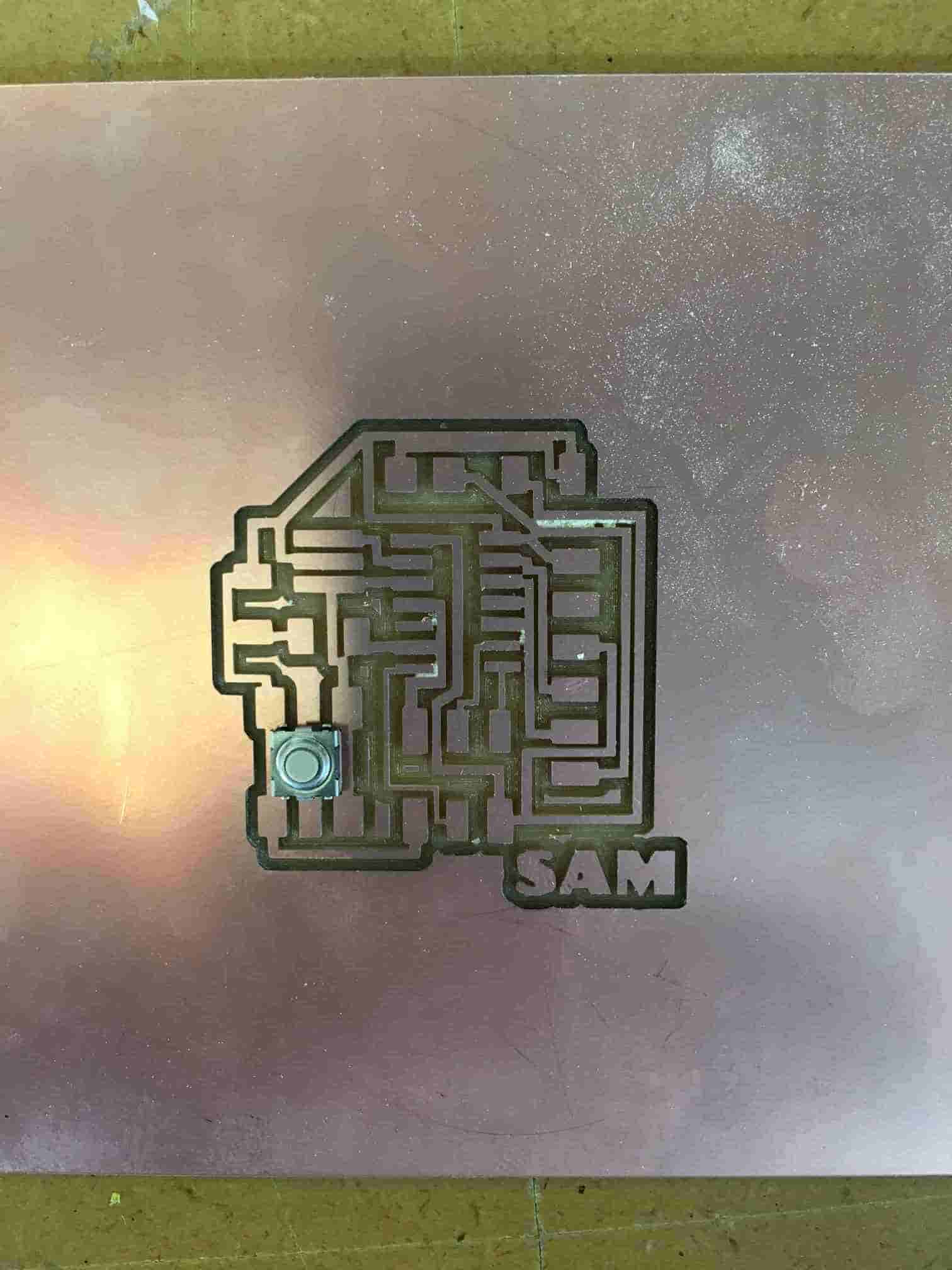
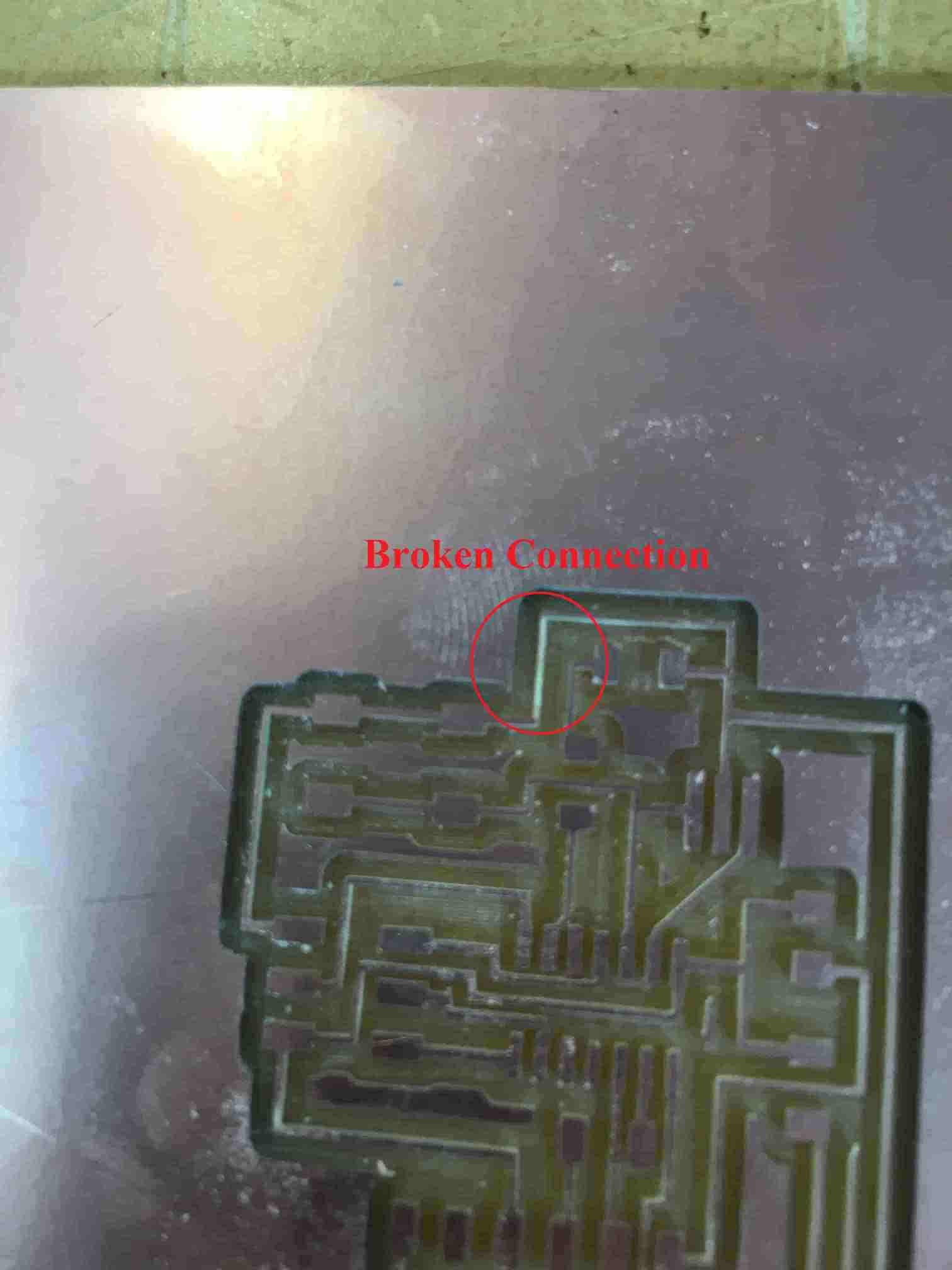
After inspection of this board, I immediately noticed problems with it. I speculated that exporting the file from Eagle threw the scale off, which caused some of the traces to overlap. The pixel size ended up being to big and ultimately made the pads too big on the board as shown in Figure 4. I also saw that there was not enough clearance between some of the connection lines on the board. This meant I needed to create a new board layout. Another process that I could have used was the Fab Modules or DRC to help in preventing the overlapping traces. Using the same process as shown in the above video I created a new board layout and milled it out. However, when I was brushing the board off I ended up breaking one of the connections. Oops. This is shown in Figure 5.
Figure 4: Scaling Off when Image was Uploaded and Milled
Figure 5: Broken Connection on Second Board
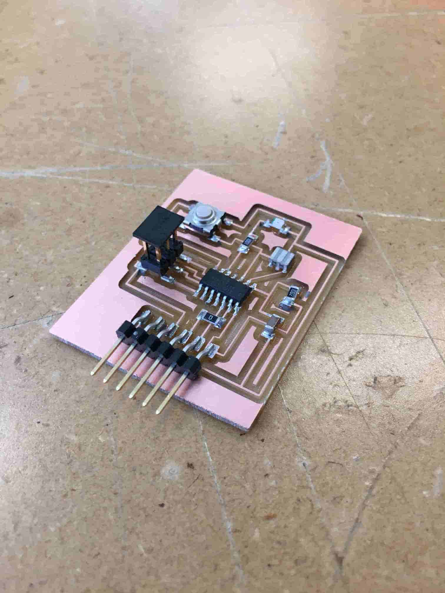
Finally, after a third attempt and being careful brushing off the board I was able to mill out a good board. I stuffed the board and tested the connections and it is now good to go for programming. The final product and traces image is shown in Figures 7 and 8.
Figure 7: Hero Shot of Board Stuffed and Ready for Programming
.jpg)